



Huawei cannot reliably win the nanometer race. So it has decided to run a different one.
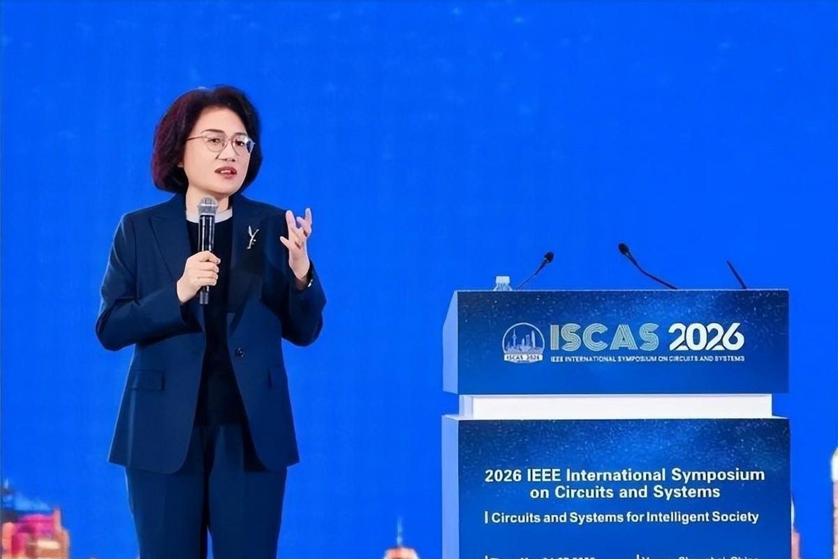
On May 25, 2026, He Tingbo, Huawei’s board member and president of semiconductor business, took the stage at the International Symposium on Circuits and Systems in Shanghai and announced what she called the τ (Tau) Law, a new principle for how chips should be made faster in an era when making transistors smaller is no longer a reliable path forward. Huawei described it as the first attempt by a Chinese company to articulate a post-Moore scaling framework with global ambitions. The announcement generated a wave of coverage, most of it focused on whether this constituted a genuine scientific contribution or a rebranding of known techniques.
Both framings miss the more consequential question: why is Huawei doing this at all, and what does it reveal about where the company is placing its bets?
The answer starts with a set of circumstances Huawei did not choose, and a moment in the industry’s trajectory that made those circumstances easier to work with.
The timing is not accidental. As transistor scaling slows globally, AI systems are becoming increasingly constrained by data movement rather than raw compute. The bottleneck is shifting from how fast a single chip can calculate to how efficiently thousands of chips can share data across a system. The industry was already moving toward advanced packaging, chiplets, and optical interconnects to address that shift. Huawei’s contribution was to turn those scattered trends into a single narrative, and claim the naming rights before anyone else did.
Since 2020, U.S.-led export controls have effectively cut Huawei off from the ecosystem required to manufacture chips at the industry’s leading edge. The result is that Huawei cannot access leading-edge manufacturing on the same terms as Apple, Nvidia, or Qualcomm. The Mate 60’s appearance of 7nm-class chips, achieved through SMIC, showed that the door is not entirely shut. But competing at the industry’s true frontier has become extraordinarily difficult in a way that is structural, not temporary.
That frontier has a straightforward competitive logic. Smaller transistors fit more computing power into the same area, consume less energy per operation, and run faster. This is what Moore’s Law predicted in 1965 and what the industry has organized itself around ever since. Every two years or so, the leading foundries push to a new node: 7nm, 5nm, 3nm. The companies that can access those nodes gain a measurable performance advantage over those that cannot.
Competing there, at the very frontier, is what Huawei cannot currently do on equal terms. That is the constraint within which the τ Law was designed.
A Different Variable to Optimize
The τ Law proposes an answer to that constraint. In Huawei’s formulation, τ refers to the effective RC time constant that governs how quickly signals can propagate and switch states within a chip. Smaller τ means faster signals, more operations per second, higher effective performance.
Moore’s Law, underneath all the transistor-count language, was always producing performance gains by reducing τ: shrink the transistors, shorten the wires connecting them, signals arrive faster. Huawei’s argument is not that this was wrong. It is that there are other ways to reduce τ that do not require a new process node: through the circuit layout, the chip architecture, and the systems connecting chips together.
Huawei defines a four-layer optimization stack: the transistor itself, the circuit connecting transistors, the chip connecting circuits, and the system connecting chips. Each layer has its own version of τ, and each offers opportunities to compress signal travel time without shrinking transistor dimensions. The τ Law is a framework for pursuing all four simultaneously.
Here is the honest assessment of what this represents: Huawei did not discover this direction. The physics pointing toward it, with RC delay as the binding constraint as geometric scaling slows, has been in semiconductor textbooks for decades. Intel, TSMC, and Samsung are all working on versions of the same techniques. What Huawei did was name the direction, formalize it into a single framework, and build a public roadmap around it. That is a different kind of contribution than inventing the underlying physics. But it is not nothing. Moore’s Law itself was not a discovery of new physics. It was a prediction that became a commitment that became a coordination mechanism for an entire industry.
Folding Is Not Stacking
The most tangible expression of the τ Law at the chip level is Logic Folding, and understanding it requires separating it from something it superficially resembles: conventional 3D chip stacking.
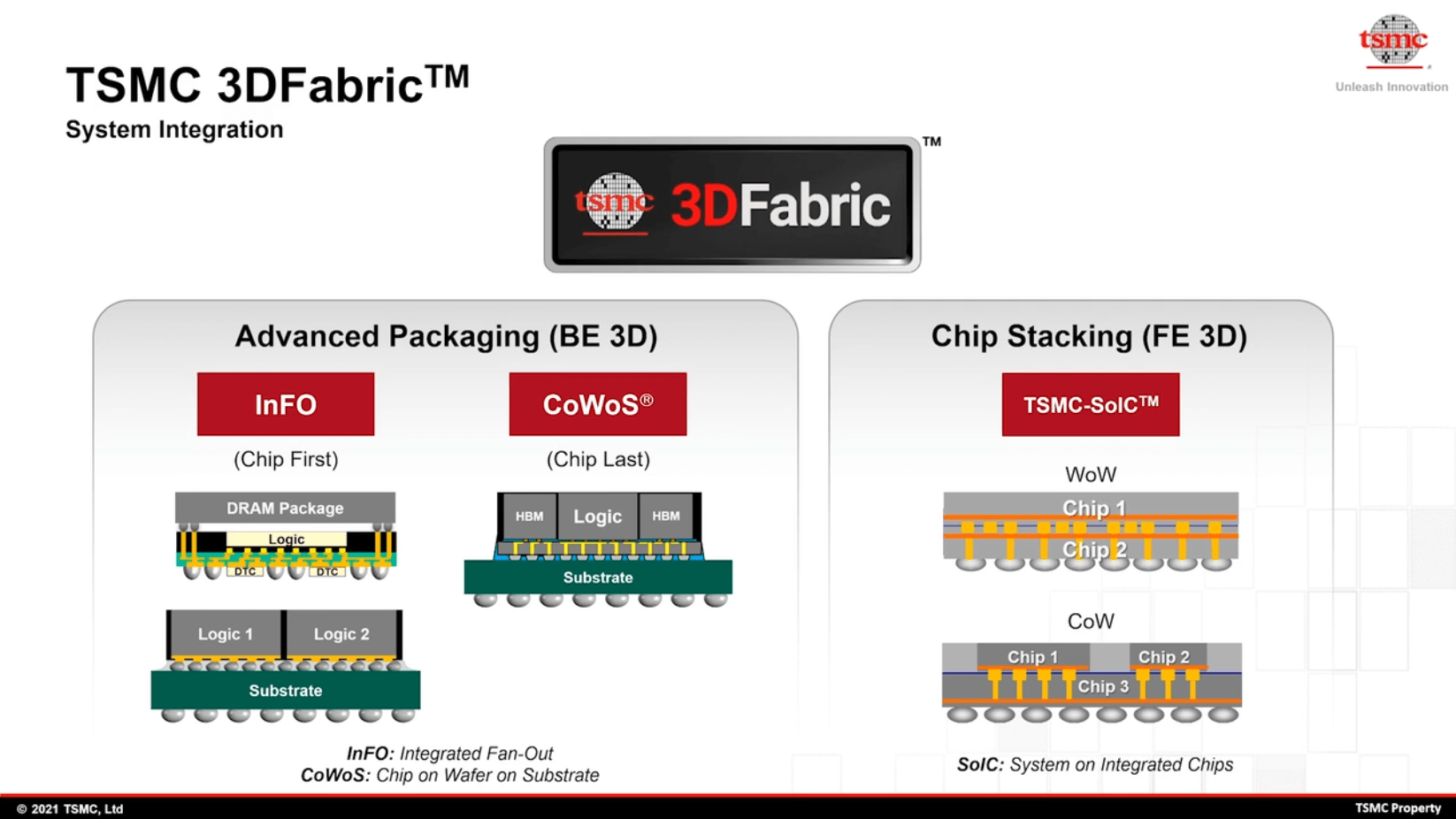
The semiconductor industry has been stacking chips for years. TSMC’s SoIC, Intel’s Foveros, and Samsung’s X-Cube all take multiple finished chips and connect them vertically to reduce the distance signals travel between them. It is a genuine and increasingly important technique. But each chip in the stack is still internally structured the same way it always was: circuits laid flat across a single layer, signals running long horizontal paths to reach neighboring gates.
Logic Folding addresses the interior of the chip, not the space between chips. Rather than finishing the chip and then connecting it to others, Huawei redesigns the circuit layout during the design phase, redistributing logic gates across multiple vertical layers within a single chip. Connections between layers are made through face-to-face hybrid bonding, routing signals vertically across short distances rather than horizontally across long ones.
3D stacking shortens the distance between chips. Logic Folding shortens the distance inside a chip. One is a packaging innovation applied after manufacture. The other is a design innovation applied before it. They address different layers of the same problem, which is also why they are complementary rather than competing.
On the first commercial implementation, the new Kirin chip expected this autumn, Huawei claims transistor density rises from 155 million to 238 million per square millimeter, and says energy efficiency improves by 41%.
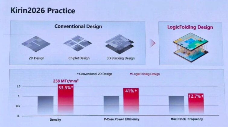
These numbers come from Huawei and have not been independently verified. What can be said without qualification is that the improvement is achieved without a new manufacturing process, on existing foundry infrastructure, which is the point the τ Law is making. The goal is approaching the transistor density associated with leading-edge nodes through design rather than fabrication.
This is a meaningful achievement if the numbers hold up. It is also, importantly, a packaging and integration achievement more than a transistor achievement. The performance gain comes from rethinking how circuit elements connect to each other, not from making them individually smaller. And that logic, followed to its conclusion at the system level, leads directly to co-packaged optics.
The Bet on Light
Logic Folding compresses τ within a chip. But modern AI systems are not single chips. They are hundreds of chips, connected across servers and racks, moving enormous volumes of data between them continuously. At that scale, the bottleneck shifts from inside the chip to between chips. The medium doing the connecting is copper wire.
Copper has worked well enough for decades, but the bandwidth demands of large AI clusters are exposing its limits. Over the distances and frequencies involved in serious AI infrastructure, copper struggles to preserve signal integrity, generates heat that compounds across thousands of interconnected chips, and draws power in quantities that have become a significant operational cost. The marginal improvements available from better copper engineering are diminishing.
Co-packaged optics (CPO) integrates optical components directly into the chip package, converting electrical signals to light pulses as early as possible in the signal path and carrying them across optical fiber. Where copper struggles, light preserves bandwidth and signal integrity over distance far more efficiently.
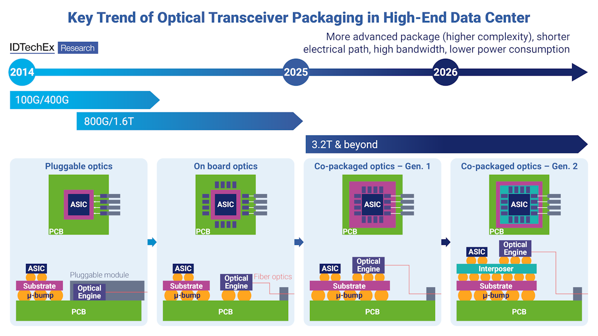
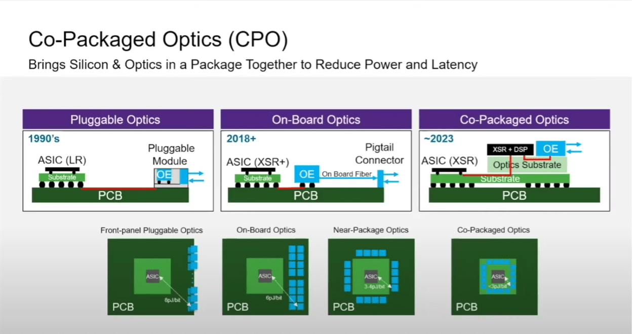
Huawei’s optical interconnect engine, Hi-ONE, targets eight terabits per second of bandwidth and compresses effective chip-to-chip signal distances from roughly a meter to five centimeters.
This is not a direction Huawei invented. According to TSMC’s April 2026 technology symposium press release, its co-packaged optics platform COUPE delivers 2x better power efficiency and 10x lower latency compared to pluggable modules on a circuit board. Nvidia has photonics-based switching products shipping this year; Broadcom is already on its third-generation CPO product. The industry has been converging on this answer for several years.
What the τ Law does is place CPO explicitly at the top of a formal optimization hierarchy: the system-level destination of the same design philosophy that Logic Folding expresses at the circuit level. Different layer, same variable being compressed. And for a company that cannot compete at the frontier of transistor fabrication, the interconnect layer represents a more accessible dimension of competition. It requires manufacturing sophistication and systems integration capability, but it does not require access to the most advanced process nodes.
The most immediate beneficiaries of this direction may not be chip designers at all, but the packaging, bonding, and optical interconnect suppliers who build the physical infrastructure that makes τ optimization possible.
Advanced packaging houses, including Changdian Technology, Tongfu Microelectronics, and Huatian Technology, sit at the intersection of every technique the τ Law describes. 2.5D and 3D integration, hybrid bonding, chiplet assembly, HBM co-packaging, and CPO integration all run through their production lines. Changdian has already raised its 2026 capital expenditure budget to roughly 10 billion yuan, up 18% from the prior year, targeting AI computing, HBM memory, and automotive packaging lines. Tongfu committed 4.22 billion yuan in April for high-performance computing and memory packaging capacity. These investments were not made in response to a speech in Shanghai. They were made in response to the same underlying forces that produced it.
The CPO supply chain sits one layer above: optical engine designers, silicon photonics foundries, fiber interconnect manufacturers. As AI clusters grow in scale, the copper-to-light transition at the system level is no longer a research topic. Guojin Securities called 2026 the first year of CPO industrialization. TSMC, Nvidia, and Broadcom have all moved into the space. The question for the packaging and photonics industries is not whether this transition happens but how fast, and who captures the most value as it does.
The Honest Accounting
There are two ways to read the τ Law, and both contain some truth.
The skeptical reading: Huawei has packaged known techniques, vertical circuit stacking, hybrid bonding, and optical interconnects, into a proprietary framework and given it a name that implies more novelty than is strictly warranted. The performance claims for the new Kirin chip come from Huawei alone and await third-party validation. The 2031 roadmap target of density equivalent to a 1.4nm node, achieved without a 1.4nm foundry, is ambitious enough to require significant skepticism.
The more generous reading: Huawei says it has developed and shipped 381 chip products across mobile, AI, automotive, and communications over the past six years. It has done so by pushing harder than most on the integration and interconnect dimensions, having been forced to rely more heavily on these approaches than companies that retain access to the most advanced process nodes. The τ Law is less a scientific discovery than a strategic declaration: a statement of where Huawei intends to compete and on what terms.
Whether the τ Law ultimately proves correct is almost beside the point. Moore’s Law was valuable not because it described new physics, but because it coordinated an entire industry around a shared roadmap, giving foundries, equipment makers, chip designers, and investors a common timeline to build toward. Huawei appears to be attempting something similar: a framework capable of organizing a parallel ecosystem around a different set of optimization targets, under very different constraints and from a very different starting point.
That may be the most significant thing that happened in Shanghai on May 25. Not a law, exactly. But possibly the beginning of one.
This is a very detailed and neutral article that gives people a better understanding of Huawei and China's computing power ecosystem. It's fantastic!